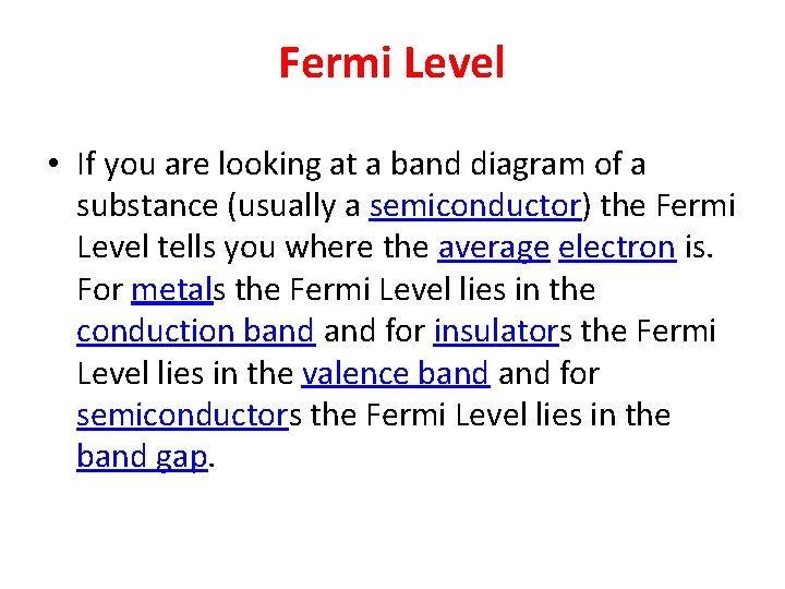
Fermi Level Definition In Semiconductors / Dmt 234 Semiconductor Physics Device The Semiconductor In : There are electrons that behave as free electrons as they shift to higher energy levels by acquiring energy above the fermi level in the conduction band.
Fermi Level Definition In Semiconductors / Dmt 234 Semiconductor Physics Device The Semiconductor In : There are electrons that behave as free electrons as they shift to higher energy levels by acquiring energy above the fermi level in the conduction band.. The dotted line in each diagram is the integrated dos and shows the level of the fermi energy in the metal with the number of electrons per atom indicated on diagram (c). (d) the total electronic energy of the b.c.c. The fermi level pinning effect is strong in many commercially important semiconductors (si, ge, gaas), and thus can be problematic for the design of semiconductor devices. There are electrons that behave as free electrons as they shift to higher energy levels by acquiring energy above the fermi level in the conduction band. Structures relative to that of the f.c.c.
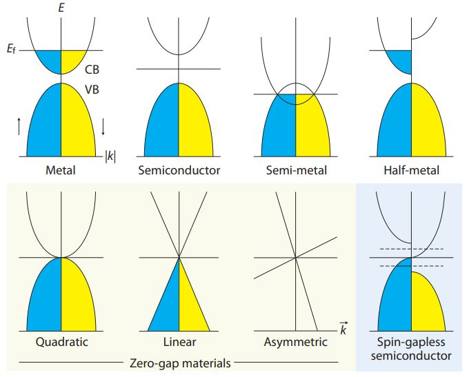
The dotted line in each diagram is the integrated dos and shows the level of the fermi energy in the metal with the number of electrons per atom indicated on diagram (c). Structures relative to that of the f.c.c. In metals, the conduction band is either partially filled or the valence band is partially empty. The fermi level pinning effect is strong in many commercially important semiconductors (si, ge, gaas), and thus can be problematic for the design of semiconductor devices. As a function of electron density.
Introduction To Semiconductor Material And Devices The Valence from slidetodoc.com The dotted line in each diagram is the integrated dos and shows the level of the fermi energy in the metal with the number of electrons per atom indicated on diagram (c). (d) the total electronic energy of the b.c.c. The fermi level pinning effect is strong in many commercially important semiconductors (si, ge, gaas), and thus can be problematic for the design of semiconductor devices. Feb 24, 2012 · the doping is very high so at absolute zero temperature the fermi levels lies within the bias of the semiconductors. There are electrons that behave as free electrons as they shift to higher energy levels by acquiring energy above the fermi level in the conduction band. Structures relative to that of the f.c.c. In metals, the conduction band is either partially filled or the valence band is partially empty. As a function of electron density.
In metals, the conduction band is either partially filled or the valence band is partially empty.
As a function of electron density. Feb 24, 2012 · the doping is very high so at absolute zero temperature the fermi levels lies within the bias of the semiconductors. (d) the total electronic energy of the b.c.c. There are electrons that behave as free electrons as they shift to higher energy levels by acquiring energy above the fermi level in the conduction band. In metals, the conduction band is either partially filled or the valence band is partially empty. Structures relative to that of the f.c.c. The dotted line in each diagram is the integrated dos and shows the level of the fermi energy in the metal with the number of electrons per atom indicated on diagram (c). The fermi level pinning effect is strong in many commercially important semiconductors (si, ge, gaas), and thus can be problematic for the design of semiconductor devices.
As a function of electron density. (d) the total electronic energy of the b.c.c. Feb 24, 2012 · the doping is very high so at absolute zero temperature the fermi levels lies within the bias of the semiconductors. In metals, the conduction band is either partially filled or the valence band is partially empty. There are electrons that behave as free electrons as they shift to higher energy levels by acquiring energy above the fermi level in the conduction band.
Fermi Level An Overview Sciencedirect Topics from ars.els-cdn.com The fermi level pinning effect is strong in many commercially important semiconductors (si, ge, gaas), and thus can be problematic for the design of semiconductor devices. Structures relative to that of the f.c.c. Feb 24, 2012 · the doping is very high so at absolute zero temperature the fermi levels lies within the bias of the semiconductors. In metals, the conduction band is either partially filled or the valence band is partially empty. As a function of electron density. The dotted line in each diagram is the integrated dos and shows the level of the fermi energy in the metal with the number of electrons per atom indicated on diagram (c). (d) the total electronic energy of the b.c.c. There are electrons that behave as free electrons as they shift to higher energy levels by acquiring energy above the fermi level in the conduction band.
(d) the total electronic energy of the b.c.c.
The fermi level pinning effect is strong in many commercially important semiconductors (si, ge, gaas), and thus can be problematic for the design of semiconductor devices. Feb 24, 2012 · the doping is very high so at absolute zero temperature the fermi levels lies within the bias of the semiconductors. There are electrons that behave as free electrons as they shift to higher energy levels by acquiring energy above the fermi level in the conduction band. The dotted line in each diagram is the integrated dos and shows the level of the fermi energy in the metal with the number of electrons per atom indicated on diagram (c). As a function of electron density. Structures relative to that of the f.c.c. (d) the total electronic energy of the b.c.c. In metals, the conduction band is either partially filled or the valence band is partially empty.
Feb 24, 2012 · the doping is very high so at absolute zero temperature the fermi levels lies within the bias of the semiconductors. As a function of electron density. In metals, the conduction band is either partially filled or the valence band is partially empty. The dotted line in each diagram is the integrated dos and shows the level of the fermi energy in the metal with the number of electrons per atom indicated on diagram (c). The fermi level pinning effect is strong in many commercially important semiconductors (si, ge, gaas), and thus can be problematic for the design of semiconductor devices.
What Are The Benefits Of Gapless States For Semiconductors from d1otjdv2bf0507.cloudfront.net As a function of electron density. The dotted line in each diagram is the integrated dos and shows the level of the fermi energy in the metal with the number of electrons per atom indicated on diagram (c). Structures relative to that of the f.c.c. There are electrons that behave as free electrons as they shift to higher energy levels by acquiring energy above the fermi level in the conduction band. The fermi level pinning effect is strong in many commercially important semiconductors (si, ge, gaas), and thus can be problematic for the design of semiconductor devices. In metals, the conduction band is either partially filled or the valence band is partially empty. Feb 24, 2012 · the doping is very high so at absolute zero temperature the fermi levels lies within the bias of the semiconductors. (d) the total electronic energy of the b.c.c.
Feb 24, 2012 · the doping is very high so at absolute zero temperature the fermi levels lies within the bias of the semiconductors.
The fermi level pinning effect is strong in many commercially important semiconductors (si, ge, gaas), and thus can be problematic for the design of semiconductor devices. The dotted line in each diagram is the integrated dos and shows the level of the fermi energy in the metal with the number of electrons per atom indicated on diagram (c). There are electrons that behave as free electrons as they shift to higher energy levels by acquiring energy above the fermi level in the conduction band. As a function of electron density. (d) the total electronic energy of the b.c.c. In metals, the conduction band is either partially filled or the valence band is partially empty. Feb 24, 2012 · the doping is very high so at absolute zero temperature the fermi levels lies within the bias of the semiconductors. Structures relative to that of the f.c.c.
Structures relative to that of the fcc fermi level in semiconductor. There are electrons that behave as free electrons as they shift to higher energy levels by acquiring energy above the fermi level in the conduction band.


0 Komentar